Semi-conductor Manufacturing Depends on Ultrasonic Cleaning Technology to Keep the World Connected
Process tooling surfaces used in semiconductor manufacturing require scheduled maintenance to decontaminate and recoat the tooling surface. Custom ultrasonic cleaning systems are the preferred method used throughout this industry by semiconductor manufacturers and third party cleaning and verification companies.


High Technology Sector Depends on Ultrasonic Cleaning to Ensure it Meets Global Demand
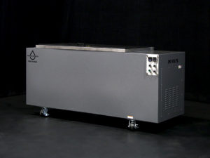
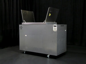
Looking to set up or add to an existing ultrasonic cleaning line for the semiconductor industry? Semiconductor and photovoltaic manufacturing requires high-end process tooling to be cleaned to ultra-high purity levels prior to coating and recoating. Properly optimized coating surfaces operate at consistent levels for longer stretches of time, providing higher yields. Ultrasonic cleaning technology provides the semiconductor industry the key tool for completing this task.
Typically, 40 kHz is the prime frequency for this application but some processes are better suited for gentler, sub-micron frequency ranges of 68 and 170 kHz. As microprocessor chips get smaller and more complex, these higher frequencies will become more vital to protecting the tooling surfaces. Omegasonics has custom ultrasonic cleaning tanks throughout the world successfully employed to meet the exacting demands of this high technology sector.
It used to take a full day to manually remove support material from some 3D parts. Now we just put the parts into the ultrasonic cleaner and do something else while they’re being cleaned. After three hours, we have nice, clean parts.
– Armen Boyajyan, Product Finishing Manager, of Stratasys Direct Manufacturing
Features.
- Decontaminates Process Deposition Tooling
- Extends parts life and MTBF
- Tooling operates longer before recoating
- Tooling operates more consistently
- Allows for better recoating adhesion
- Faster chamber start-ups

